

Flexible Work
Cloud-Based
New interface, web-based tool, high efficiency, no need to download. AWS ensures data security.
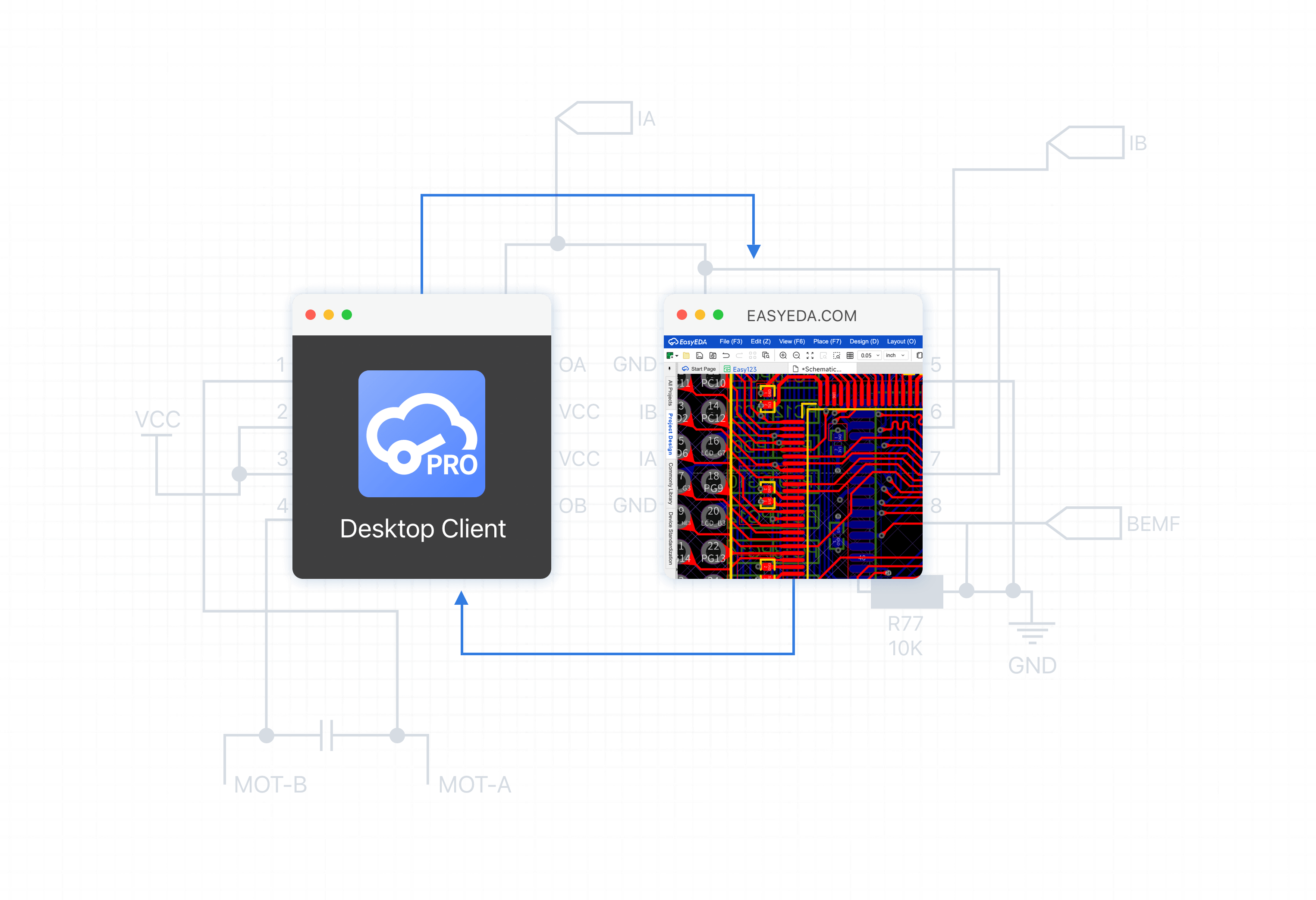
Desktop Client
EasyEDA desktop client has offline and semi-offline modes that support local storage of all projects.
On Premises Hosting
Data is securely stored on dedicated enterprise servers, enabling support for a larger enterprise user base and ensuring rapid processing and storage of vast amounts of data.
Multi-platform Compatibility
Supports AMD64, SW_64, ARM64, LoongArch64, and other CPU architectures.
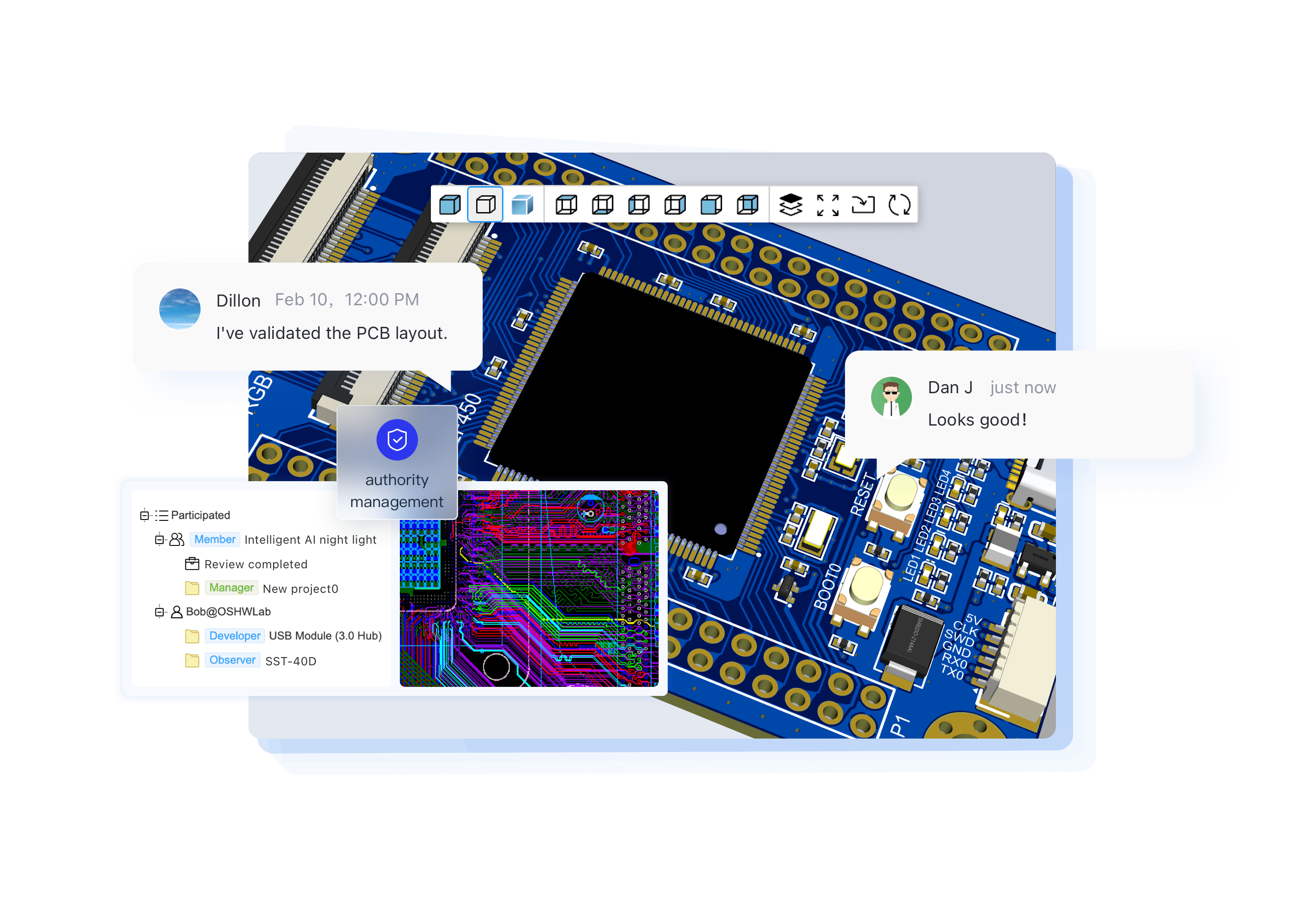
Team Work
Team Role
Team roles are categorized as Managers, Developers, and Observers, streamlining tasks and boosting security through clear role definitions.
Team Data
All project data, including projects, libraries, and models, will be owned by the team and can be uploaded as team documents.
Real-time Control
Manage team members and data in real-time. You can easily view all team project status and logs in the workspace.
Efficient Co-Design
Allow multiple designers to collaborate effortlessly from any location or device, empowering teams to comment on designs and enhance teamwork effectiveness.
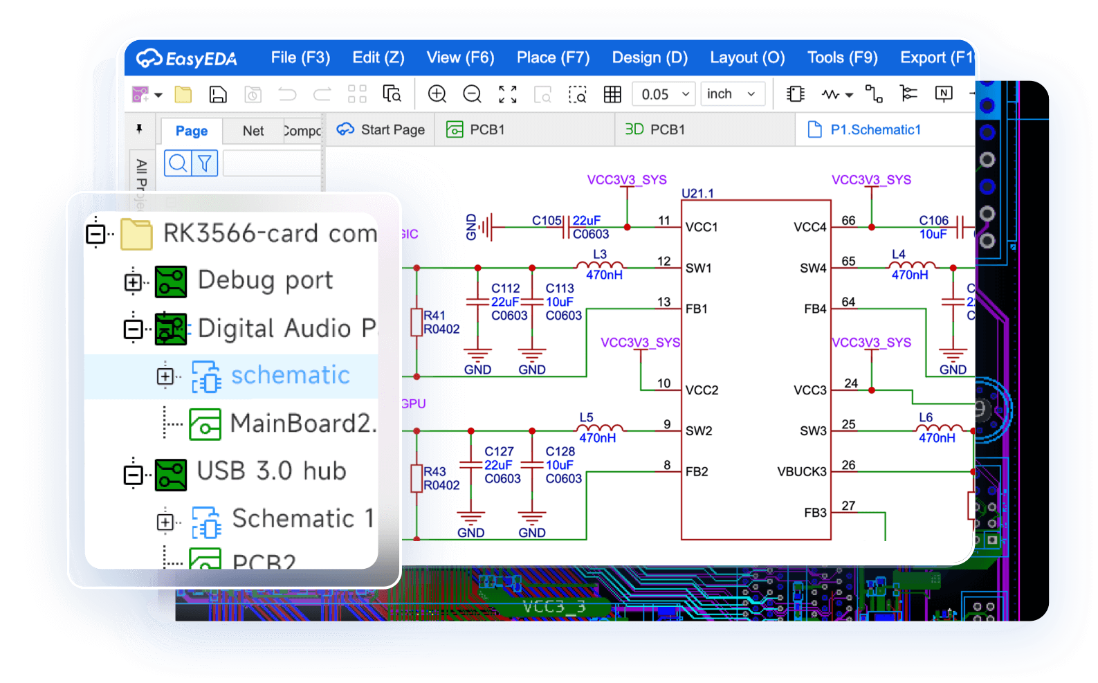
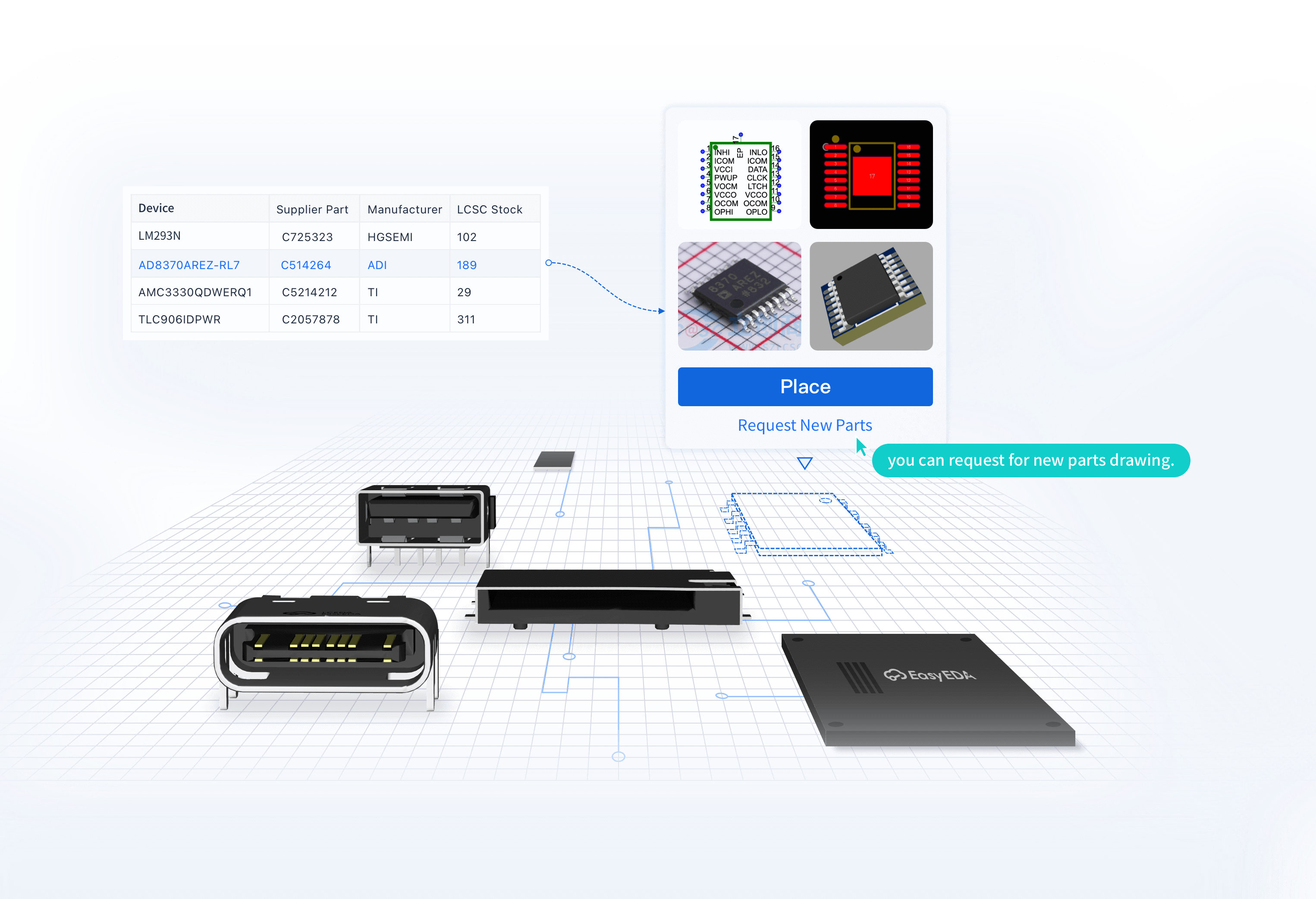
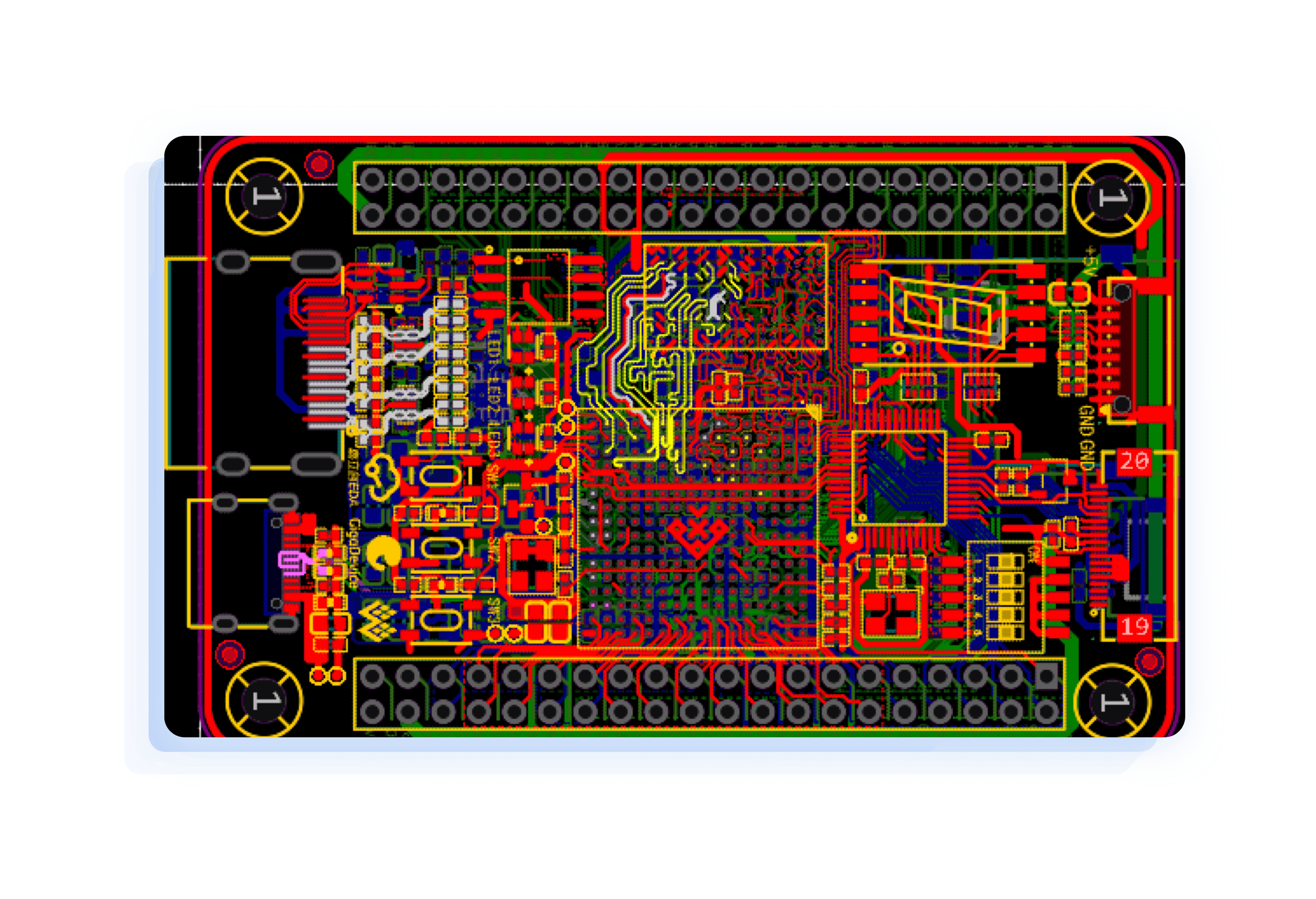
Advanced Library Management
Device Manager
Easily replace components using the Device Manager, allowing for quick modification of component properties and standardized BOM output.
Component Request for Free
If you can't find the components you need in the library, submit a request and EasyEDA will create the library drawings for you free of charge.
Device Standardized
Visualization tools help users check component information and manage BOM in real-time. Whether updating or replacing, the components used in the project are clear at a glance.
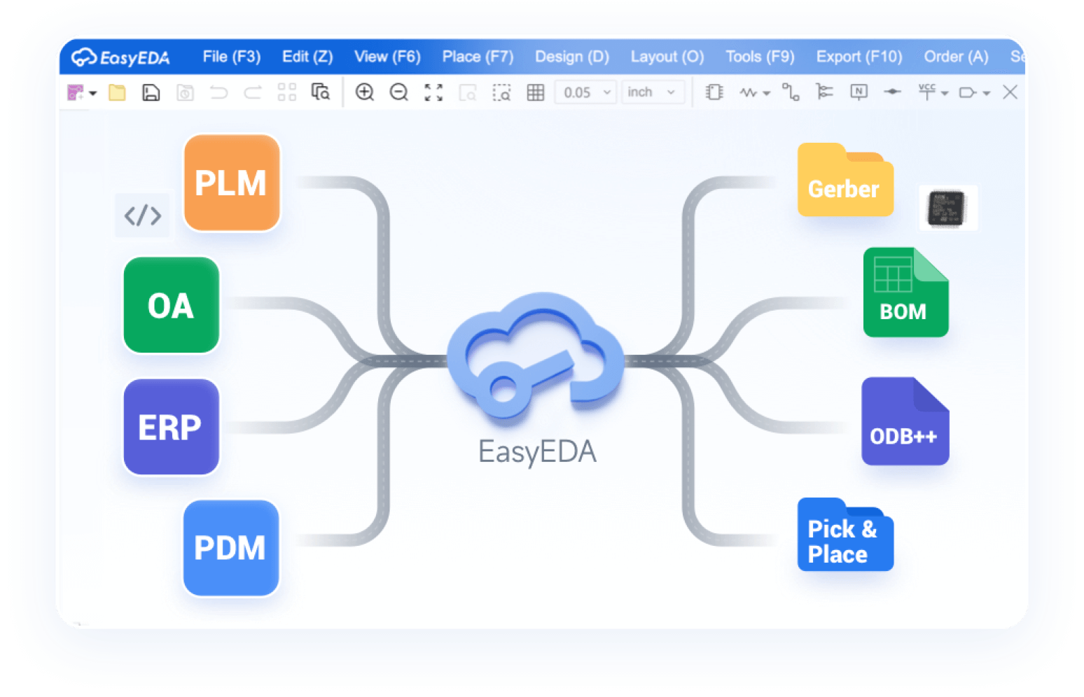
ERP/PLM Data Connection
EasyEDA allows connecting to ERP/PLM systems. You can use PLM's real-time material data, such as price, inventory, etc., to complete the parts selection during the design process.
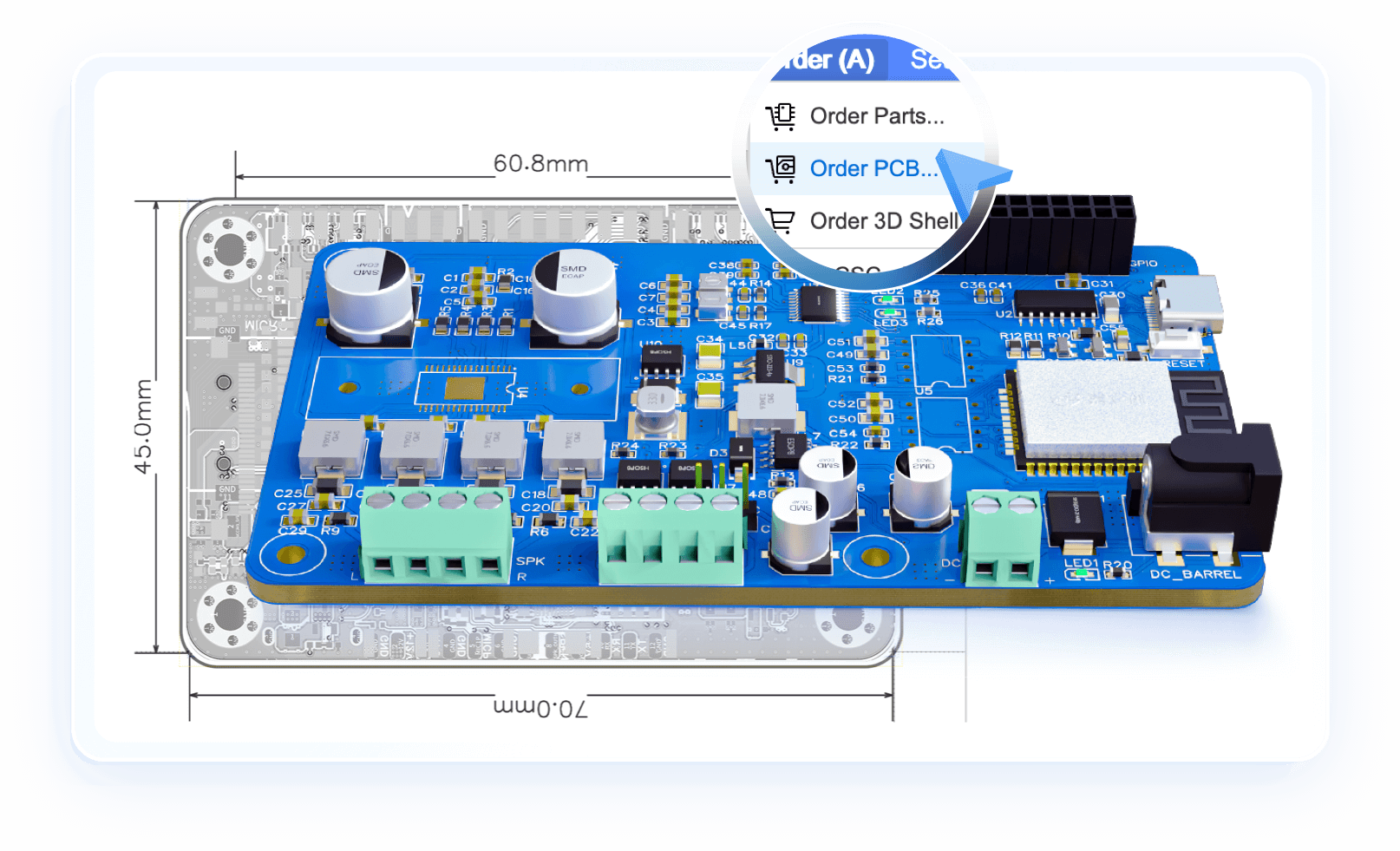
Layout Services
Design Visualization
View the progress of designs anytime, intuitive and clear.
Competitive Price
Enjoy competitive pricing at $0.5 per pin, a project with 3000 pins can be completed within 5 days. Also supports PCB layout designs with over 100,000 pins.
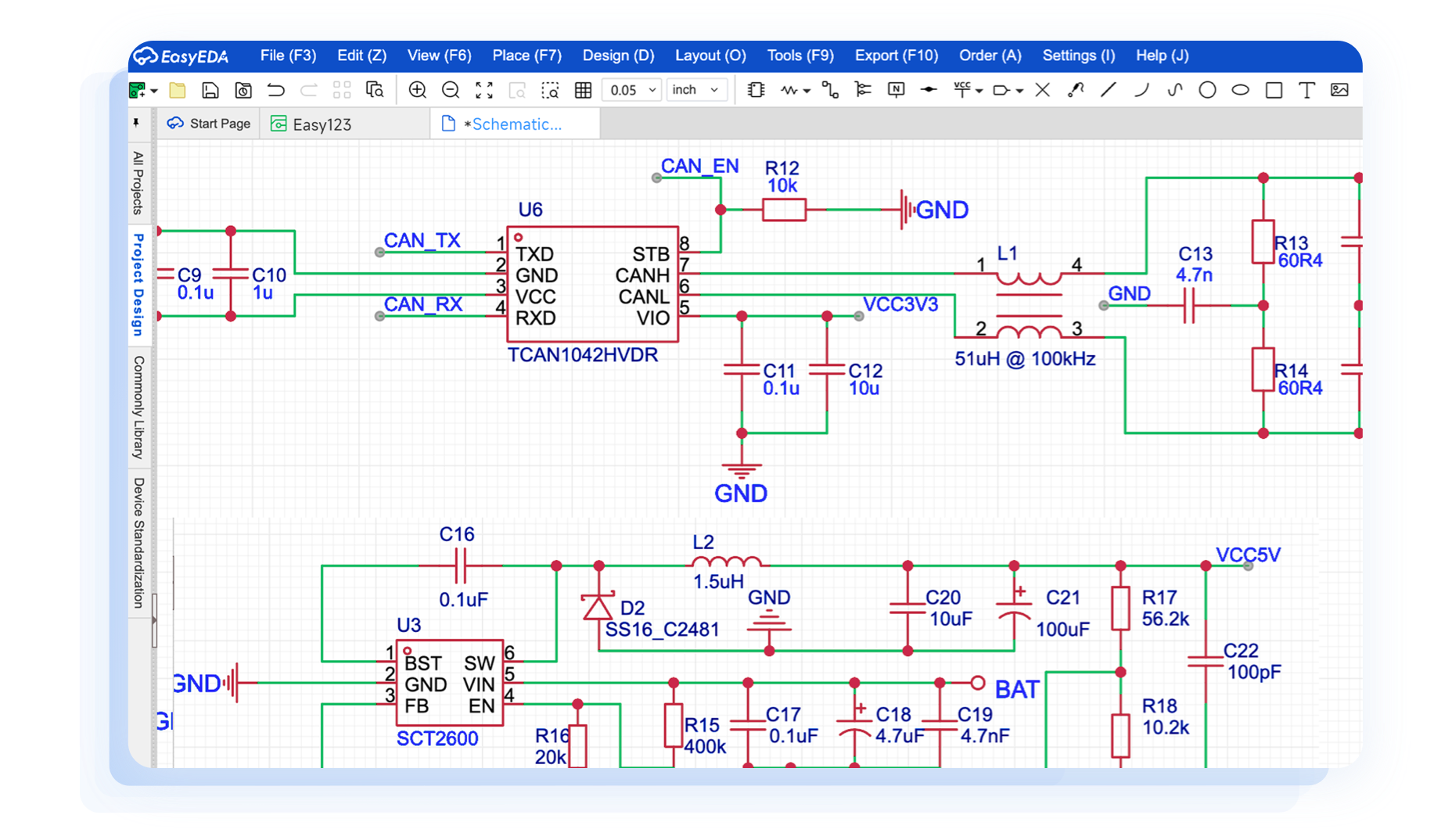
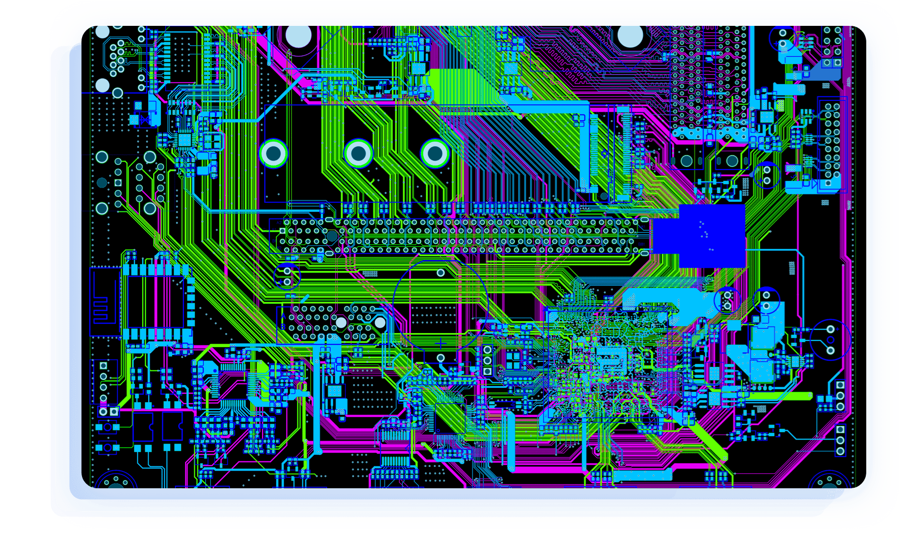
Support for Complex Designs
Supports high-frequency, high-speed, FPC, and high power PCB design.
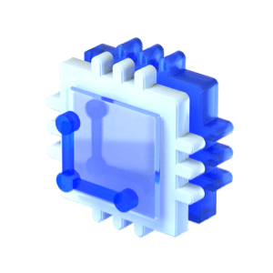
3D Model Library
Use EasyEDA design to swiftly generate a free 3D structure of your PCB, streamline the structural design process, and export STEP files quickly.
Data Security
Secure your designs with AES encryption, prevent data leaks, and protect project data with multiple backups and disaster recovery.


 Brand new interactions and interfaces.


 Easy to use and quick to get started.